双金属导体界面科学
Interface Science in Bimetallic Conductors
1. Introduction
1.1 界面作为独立section
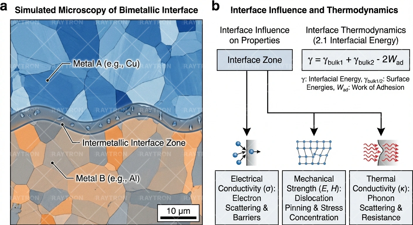
双金属导体中的界面不仅仅是两相之间的边界——它是一个具有独特性质的独立section:
创建界面section三维模型,可旋转查看原子结构
0:301.2 在双金属导体中的重要性
界面影响:
2. Interface Thermodynamics
2.1 界面能
金属-金属界面的能量可表示为:
其中:
- γA, γB = 金属A和B的Surface能
- Wad = 粘附功
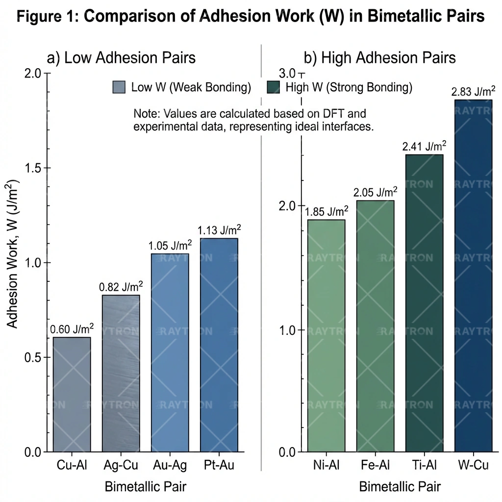
2.2 粘附功
粘附功代表分离界面所需的能量:
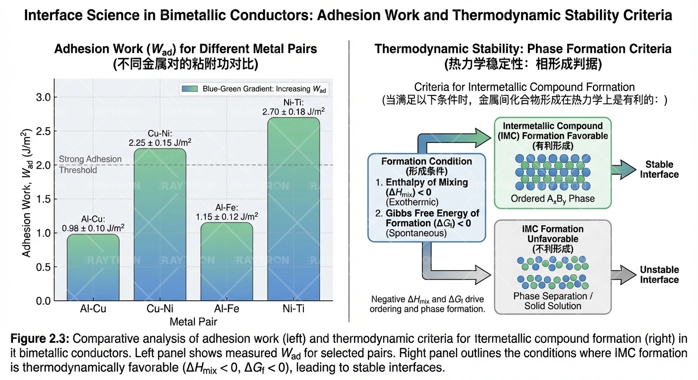
2.3 热力学稳定性
相形成判据:
当满足以下条件时,金属间化合物形成在热力学上是有利的:
3. Atomic Structure
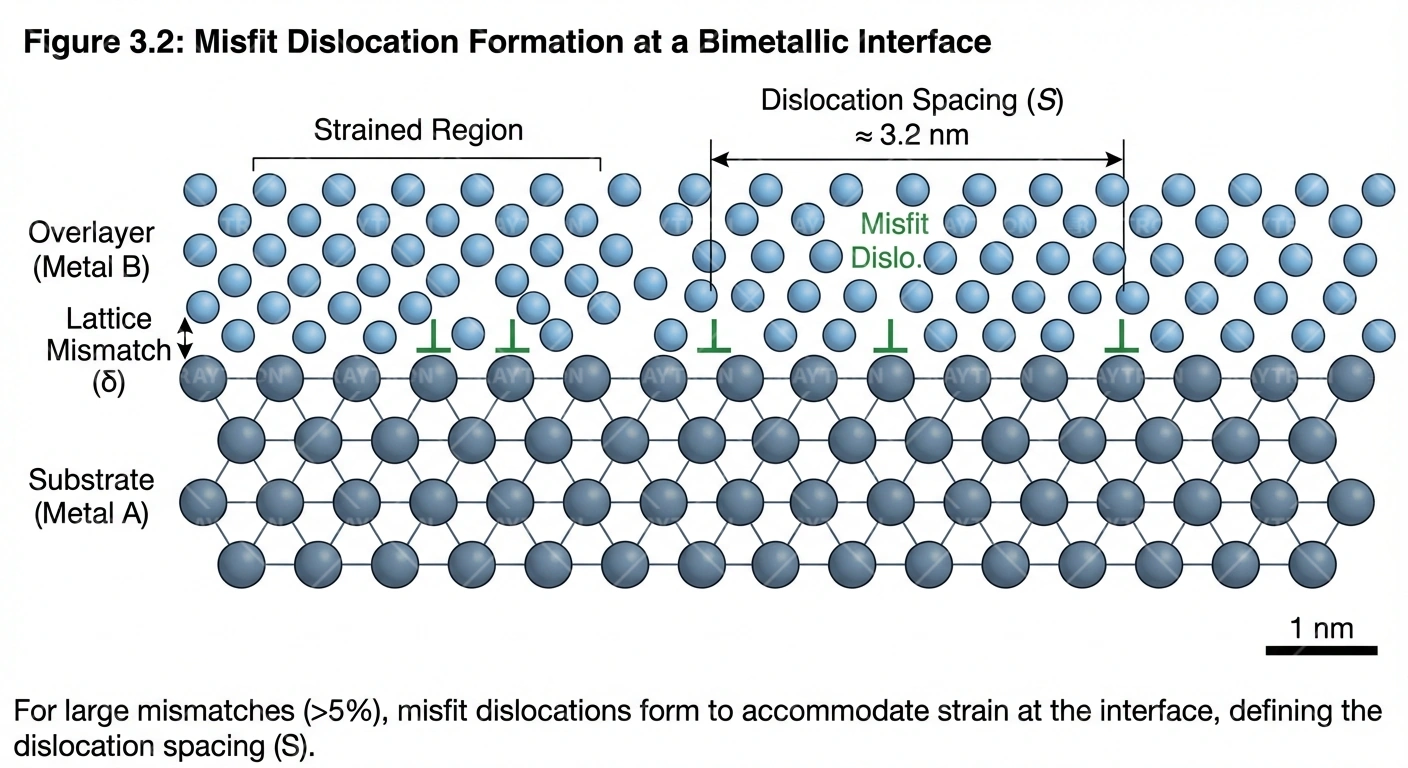
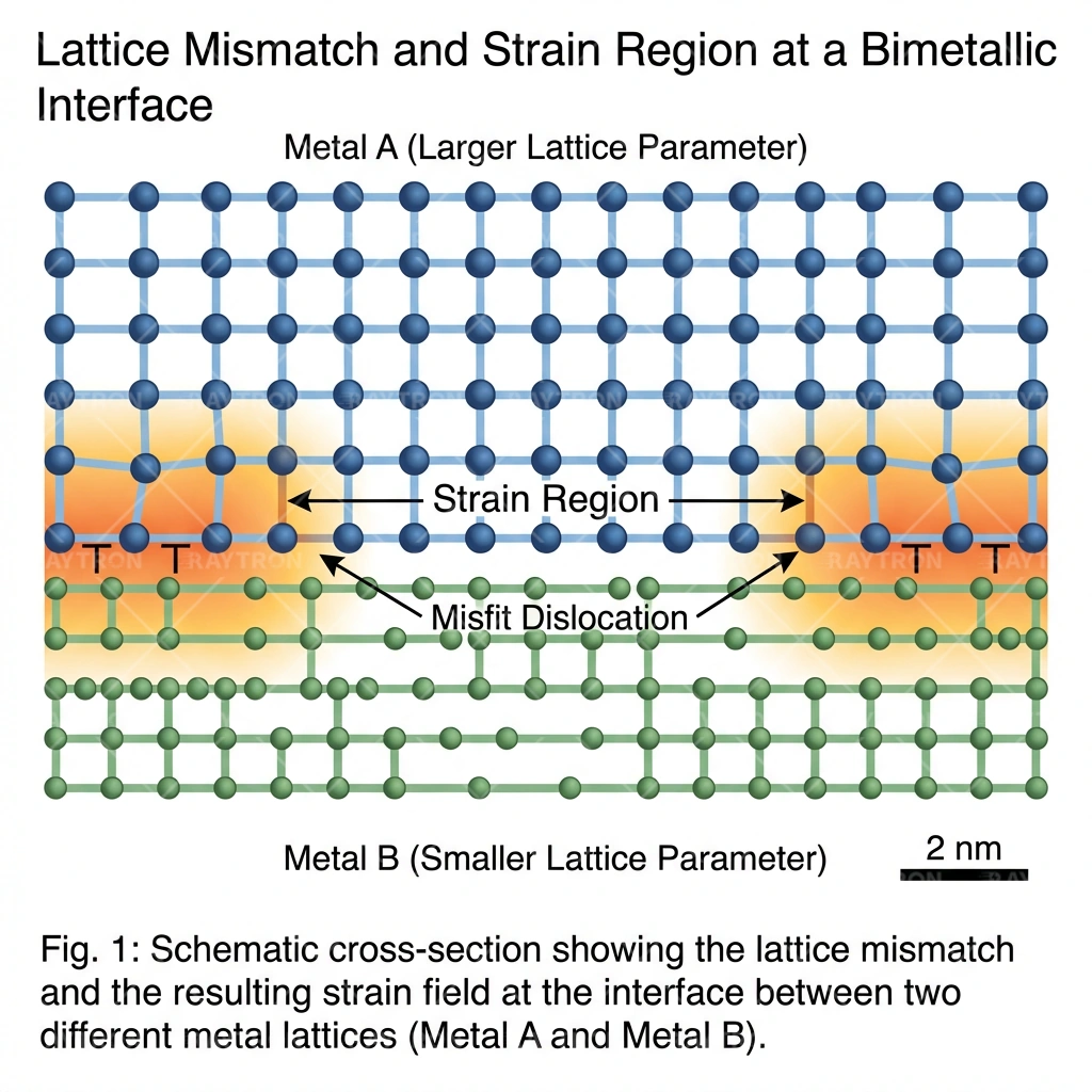
3.1 晶格失配
当两种不同晶格参数的金属相遇时,原子错配产生应变:
其中aA和aB是晶格参数。
3.2 失配位错
对于大失配(>5%),失配位错容纳应变:
创建失配位错形成动画
0:20位错间距:
其中b = 伯格斯矢量大小。
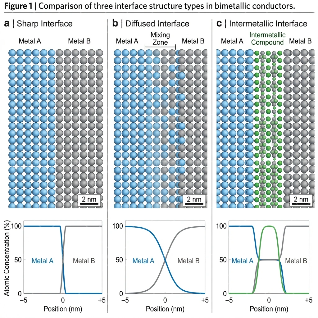
3.3 界面结构
三种界面结构类型:
4.
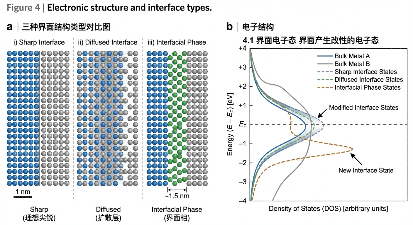
4.1 界面电子态
界面产生改性的电子态:
关键效应:
- 能带弯曲:费米能级对齐
- 界面态:局域电子态
- 电荷转移:由电负性差异引起
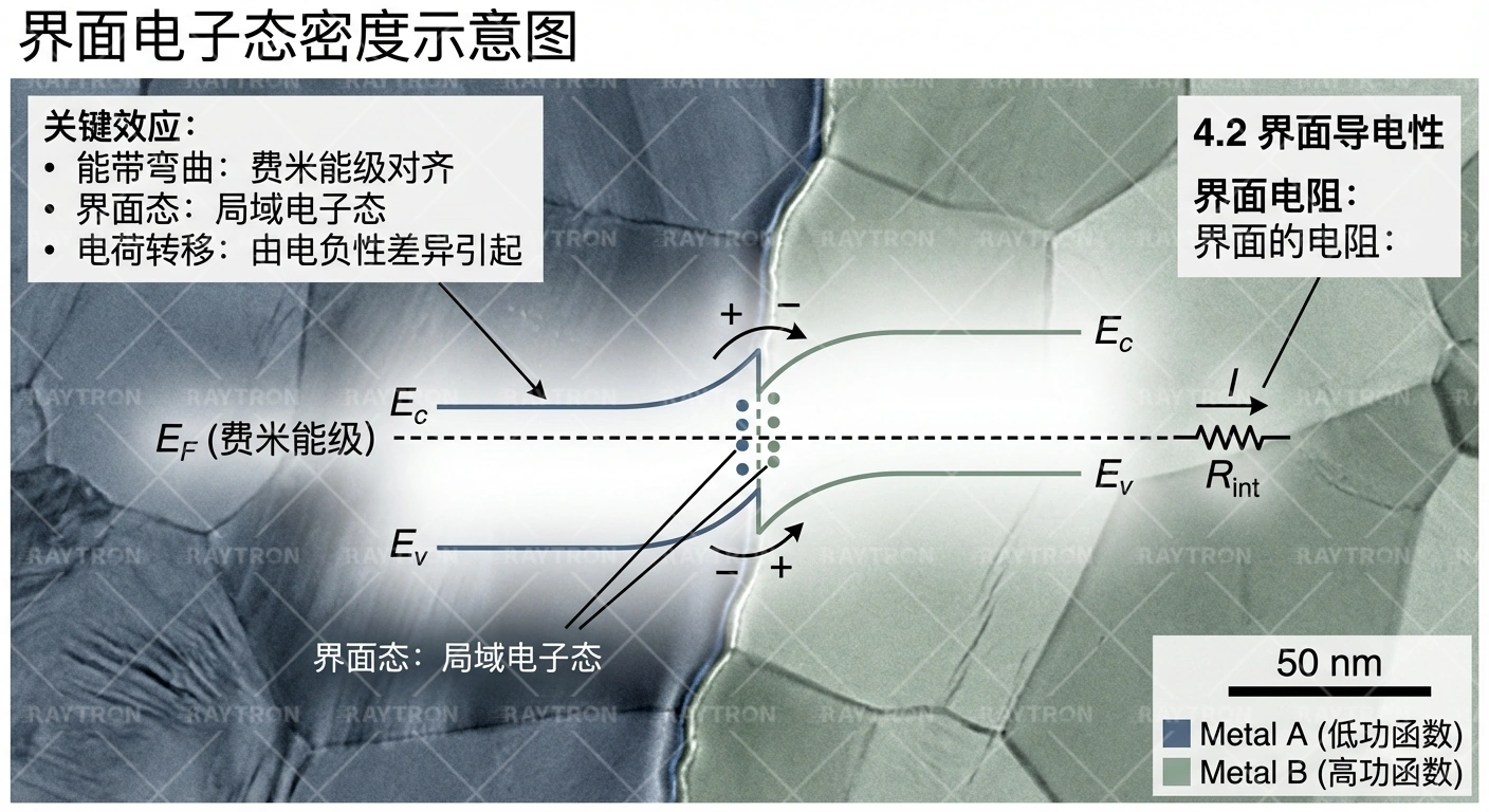
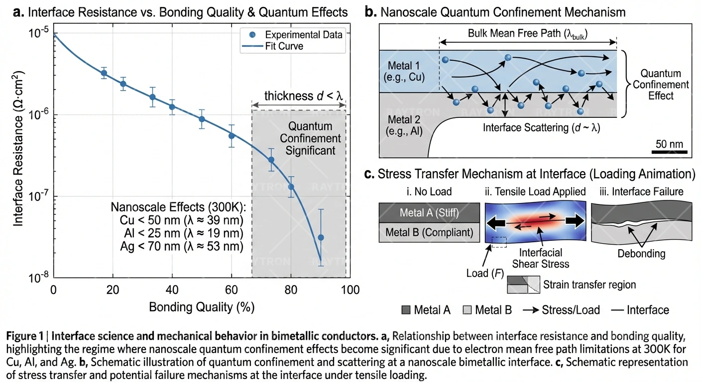
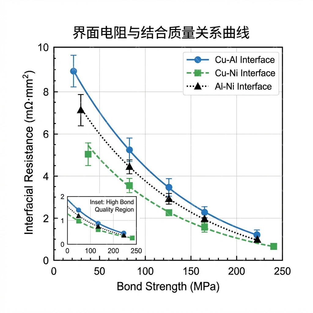
4.2 界面导电性
界面电阻:
界面的电阻:
4.3 纳米尺度量子效应
对于极薄层,量子限域效应变得显著:
平均自由程考虑:
- Cu: 39 nm (300K) - 对<50 nm层显著
- Al: 19 nm (300K) - 对<25 nm层显著
- Ag: 53 nm (300K) - 对<70 nm层显著
5.
5.1 应力传递机制
界面实现层间载荷传递:
创建应力传递动画,展示加载时界面如何传递应力
0:30剪切滞后模型:
特征长度上的应力传递:
其中:
- τ = 界面剪应力
- P = 施加载荷
- d = 直径
- Lt = 传递长度
5.2 界面强度
理论强度:
其中Eeff是有效模量。
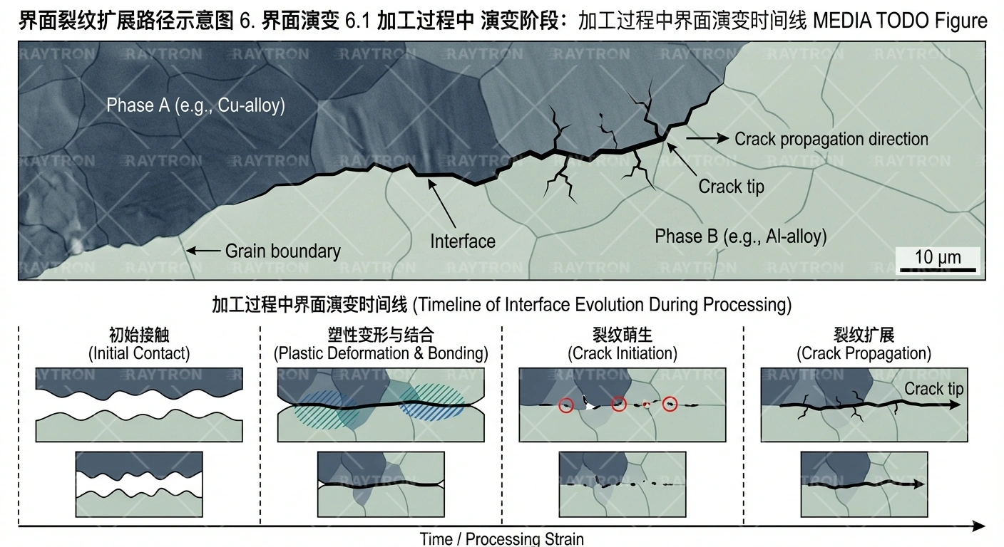
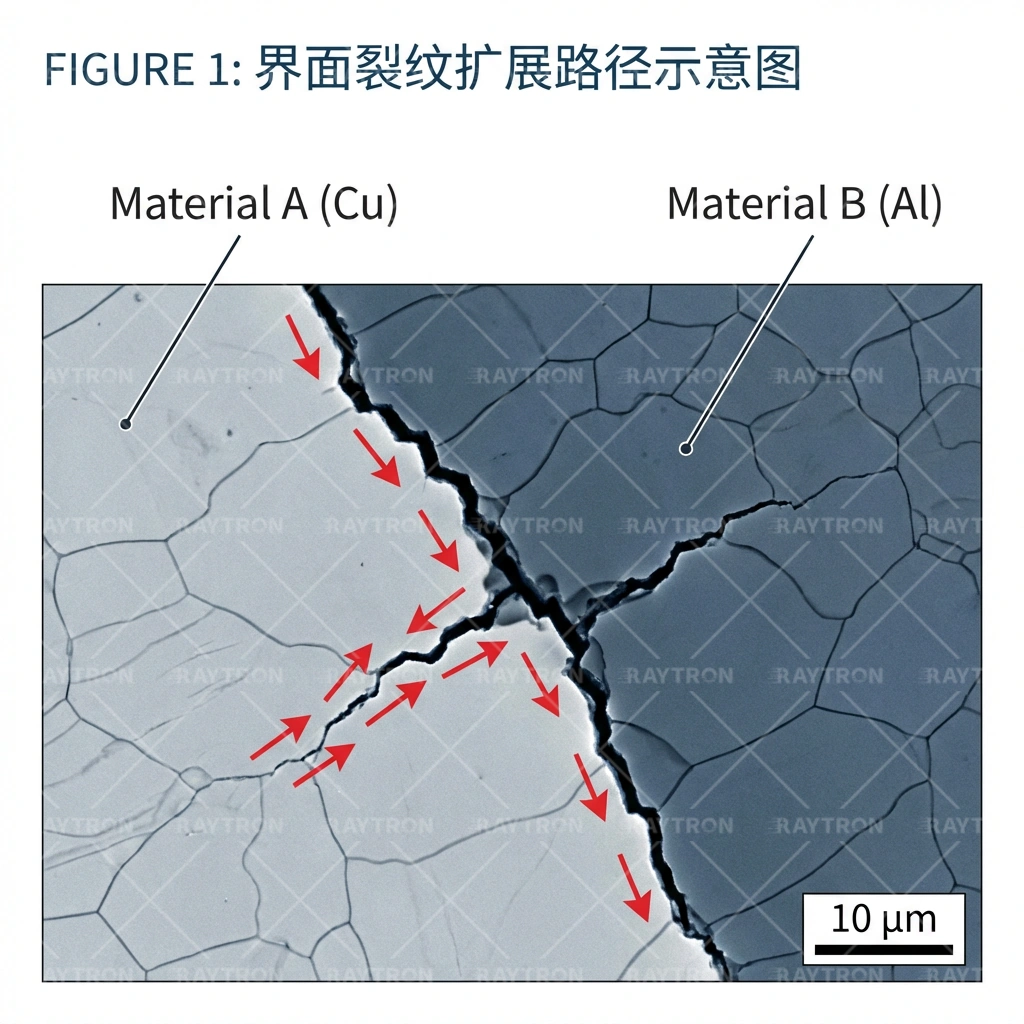
5.3 断裂行为
界面裂纹扩展:
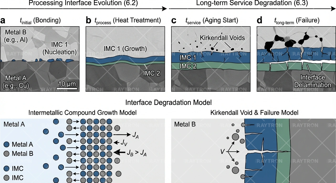
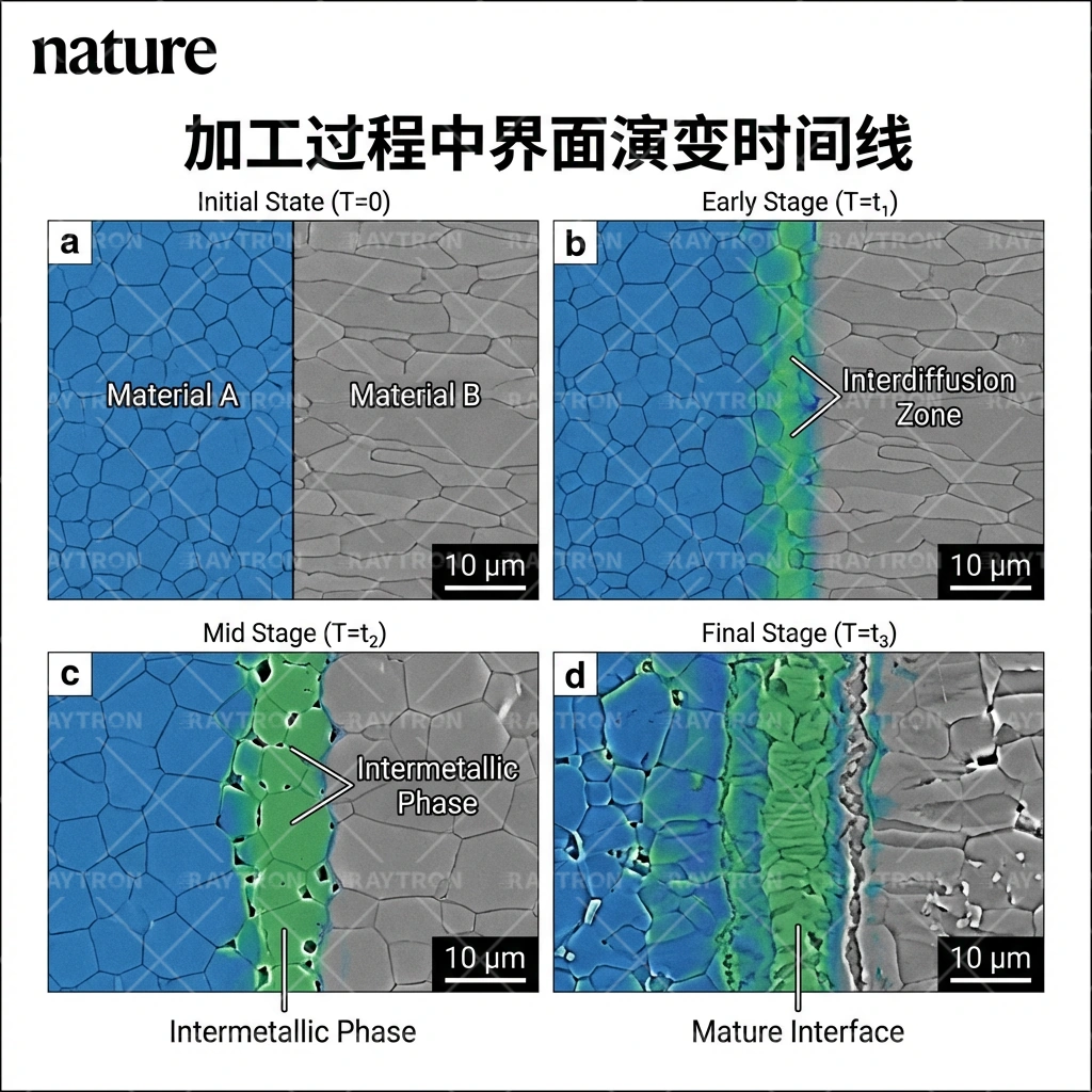
6. Interface Evolution
6.1 加工过程中
演变阶段:
6.2 服役过程中
长期演变:
6.3 界面退化模型
金属间化合物生长模型:
其中k通过阿伦尼乌斯关系取决于温度。
150°C服役温度下预测的IMC厚度:
- 1年: 0.3 μm
- 5年: 0.7 μm
- 10年: 1.0 μm
- 25年: 1.5 μm
7. Characterization
7.1 显微方法
7.2 光谱方法
EDS线扫描分析:
7.3 力学测试
纳米压痕:
8. Modeling Methods
8.1 原子模拟
分子动力学:
Applications:
- 界面能计算
- 位错结构预测
- 变形机制研究
8.2 连续介质模型
有限元分析:
界面建模方法:
- 完美结合(共享节点)
- 内聚区模型
- 接触单元
8.3 多尺度方法
9.
9.1 设计指南
9.2 质量控制指标
SPC参数:
- 界面电阻 (μΩ·cm²): USL 0.5, 目标 0.2
- 剥离强度 (MPa): USL 70, 目标 55, LSL 40
- IMC厚度 (μm): USL 3.0, 目标 2.0
- 结合覆盖率 (%): USL 100, 目标 98, LSL 95
9.3 未来方向
研究重点:
- 原位表征:实时观察界面演变
- 先进建模:机器学习加速性能预测
- 工程化界面:原子尺度设计
- 新材料组合:超越现有体系
FAQ
界面宽度对双金属导体性能有何影响?
界面宽度影响电子散射和应力传递。过宽的界面(>100nm)会增加电阻,过窄的界面(<1nm)可能导致结合强度不足。最佳界面宽度为1-10nm,可实现低电阻和High strength的平衡。
如何表征双金属界面的质量?
主要表征方法包括:SEM/TEM观察界面形貌和原子结构、EDS线扫描分析成分分布、剥离测试测量结合强度、四探针法测量界面电阻。综合这些方法可全面评估界面质量。
界面在服役过程中会发生什么变化?
高温环境下界面会发生扩散,导致金属间化合物生长;热循环会产生疲劳应力;电流通过可能引起电迁移。这些变化是缓慢的,在正常工作条件下,高质量界面可保持25年以上稳定。
为什么Cu/Ni界面比Cu/Al界面更稳定?
Cu和Ni形成连续固溶体,无脆性金属间化合物形成;晶格失配小(2.6%),界面应力低;扩散激活能高,高温稳定性好。而Cu/Al界面会形成多种脆性金属间化合物,需要严格控制加工温度。
图表
Interface Impact Schematic Diagram, Showing on Conductive、Mechanical、Hot Performance Impact
Intermetallic CompoundFormationFree Energy Diagram
LatticeMismatch Schematic Diagram, Showing StrainArea
Three Types Interface Structure Typevs Diagram
InterfaceElectronStateDensity Schematic Diagram
Interface Resistance vs Bonding QualityRelationship Curve
Interface Crack扩展Path Schematic Diagram
Processing Process in Interface Evolution Timeline
IMCGenerationLong Curve,Different Temperature under
TEM Interface DiagramImage, Annotated Differentsection
TypicalEDSWireScanning Results
InterfaceNano Press痕 Test Schematic Diagram
MDModeling Interface Structure截 Diagram
Multiscale Modeling Framework Diagram
表格
| Characteristic | Bulk Material | Interface Region |
|---|---|---|
| Atomic Arrangement | Regular Crystal | Disordered/Distorted |
| Composition | Uniform | Gradient |
| Electronic Structure | Bulk Band | Modified State |
| Stress State | Residual Stress | |
| Width | Non-Applicable | 1-100 nm |
| Metal | SurfaceCapacity (mJ/m²) | Crystal Plane |
|---|---|---|
| Cu | 1.79 | (111) |
| Cu | 1.93 | (100) |
| Al | 1.14 | (111) |
| Al | 1.35 | (100) |
| Ni | 2.01 | (111) |
| Fe | 2.48 | (110) |
| Metal on | W_ad (mJ/m²) | KeySpecial Properties |
|---|---|---|
| Cu/Al | 520 | MetalKey+some IonicKey |
| Cu/Ni | 780 | MetalKey(Electric PropertiesPhase近) |
| Cu/Fe | 620 | MetalKey |
| Al/Fe | 480 | MetalKey |
| Ag/Cu | 680 | MetalKey |
| Compound | ΔG_formation | ThermodynamicsStable? |
|---|---|---|
| CuAl₂ | -35 | is |
| Cu₉Al₄ | -28 | is |
| NiAl | -118 | is |
| FeAl | -52 | is |
| Metal on | a_A (Å) | a_B (Å) | Mismatch (%) |
|---|---|---|---|
| Cu/Al | 3.615 | 4.050 | -10.7% |
| Cu/Ni | 3.615 | 3.524 | +2.6% |
| Cu/Fe (fcc) | 3.615 | 3.591 | +0.7% |
| Al/Fe (bcc) | 4.050 | 2.866 | +41.2%* |
| Interface | Mismatch | Pitch (nm) |
|---|---|---|
| Cu/Al | 10.7% | 3.4 |
| Cu/Ni | 2.6% | 14.0 |
| Cu/Fe | 0.7% | 52.0 |
| Interface Quality | R_interface (μΩ·cm²) | on Total ResistanceImpact |
|---|---|---|
| Excellent | <0.1 | <1% |
| Good | 0.1-0.5 | 1-3% |
| General | 0.5-2.0 | 3-10% |
| ComparativelyPoor | >2.0 | >10% |
| Material | σ_bulk (MPa) | σ_interface (MPa) | RatioExample |
|---|---|---|---|
| CCA | 180 (AlCore) | 45-65 | 25-36% |
| CCS | 450 (Steel) | 50-70 | 11-16% |
| NCC | 230 (CuCore) | 55-75 | 24-33% |
| Environment | Mechanism | Effect | TimeScale |
|---|---|---|---|
| High Temperature | Diffusion | IMCGenerationLong | 1000s-10000s h |
| HotCycle | CTENon-Matching | Fatigue | 100s-1000sCycle |
| Current | Electric Migration | Composition Variation | CountYear |
| Corrosion | Galvanic | InterfaceErosion | CountYear |
| Technique | Scale | Info | 制备 |
|---|---|---|---|
| OM | >1 μm | Layer Structure、 Defects | PolishingCross-Section |
| SEM | 10 nm-1 μm | Interface Morphology | PolishingCross-Section |
| TEM | 0.1-100 nm | Atomic Structure | FIBReducedThin |
| HRTEM | <1 nm | Atomic柱 | FIBReducedThin |
| STEM-EDS | 1-10 nm | Composition Distribution | FIBReducedThin |
| Method | TestingLimit | 空间分辨Rate | Info |
|---|---|---|---|
| EDS | 0.1 wt% | 1 μm | Main Element |
| WDS | 0.01 wt% | 1 μm | 微量Element |
| 俄歇 | 0.1 at% | 50 nm | Surface Composition |
| XPS | 0.1 at% | 10 μm | 化学State |
| MaterialSystem | 势函Count | System Dimension | TimeScale |
|---|---|---|---|
| Cu/Al | EAM | 10⁶ Atomic | 10 ns |
| Cu/Ni | EAM | 10⁵ Atomic | 1 ns |
| Cu/Fe | MEAM | 10⁵ Atomic | 1 ns |
| Requirements | Parameter | Target |
|---|---|---|
| Low Resistance | R_interface | <0.5 μΩ·cm² |
| High strength | Peel Strength | >40 MPa |
| Stability | IMC Thicknessss | <3 μm |
| Uniform Properties | Bonding覆盖Rate | >95% |
参考文献
- Surface free energies of solid metals Surface Science 62(1) , 267-276 (1977)
- Interfaces in Crystalline Materials Oxford University Press (1995)
- Interfaces in Materials Wiley (1997)
- Atomic structure of Cu/Al interfaces Physical Review B 64 , 045418 (2001)
- Grain boundary diffusion in metals Defect and Diffusion Forum 323 , 1-12 (2012)
- Theory of Dislocations (2nd ed.) Wiley (1982)
- Electronic Structure of Materials Oxford University Press (1996)
- Interface characterization in bimetallic wires Materials Characterization 152 , 148-158 (2019)
- In-situ TEM study of interface evolution Acta Materialia 185 , 175-185 (2020)
- Interface Analysis of High-Performance CCA Internal Report TR-2025-012 (2025)
